This is an old revision of the document!
Table of Contents
| Start | End | Description |
|---|---|---|
| 0x000000 | 0x0027FF | RAM |
| 0x002800 | 0x002FFF | PPU |
| 0x003000 | 0x0037FF | Sound |
| 0x003D00 | 0x003DFF | IO |
| 0x003e00 | 0x003E03 | DMA |
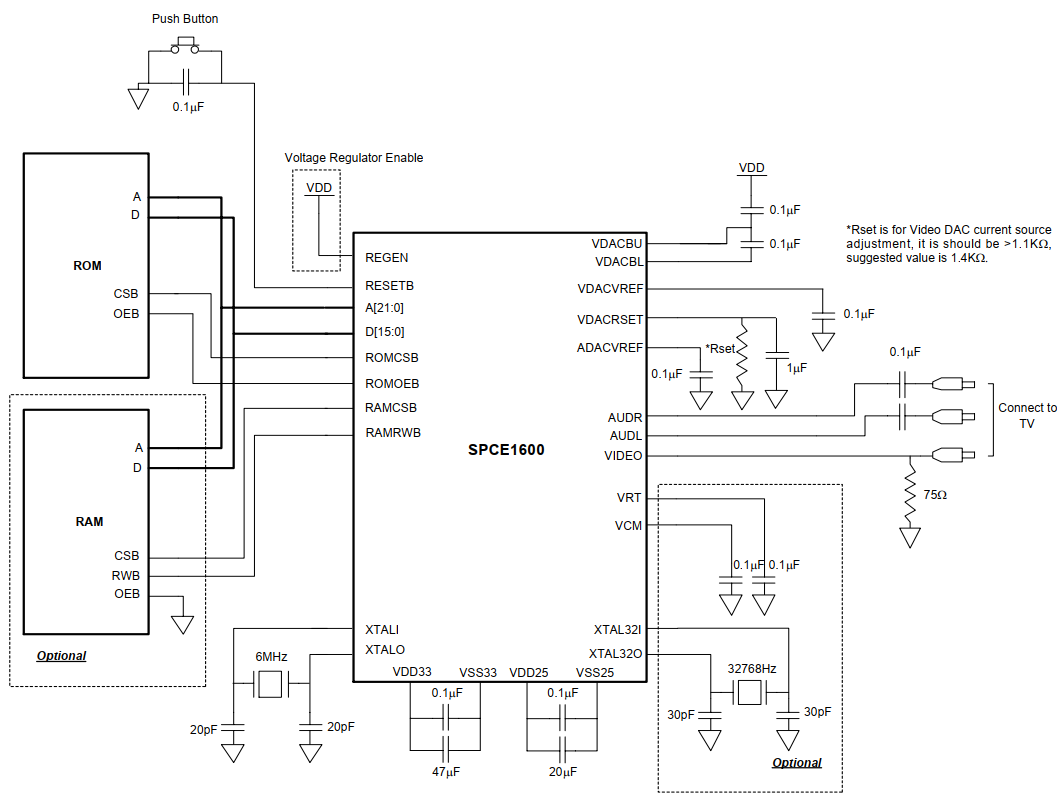
External memory starts at 0x4000. It can be mapped to the internal ROM and the two possible chips in the cartridges.
 Document how to manipulate the banking (using GPIOs?)
IO registers
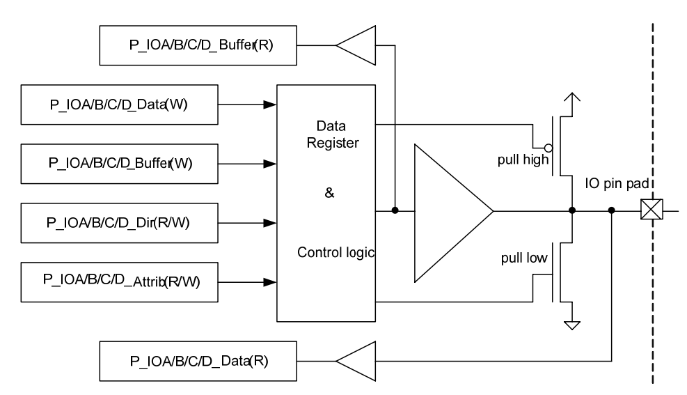
| Address | Contents |
|---|---|
| 3D00 | IO configuration |
| 3D01-3D05 | IOA registers |
| 3D06-3D0A | IOB registers |
| 3D0B-3D0F | IOC registers |
| 1/6/B | IOx data |
| 2/7/C | IOx buffer |
| 3/8/D | IOx direction |
| 4/9/E | IOx attributes |
| 5/A/F | IOx mask |
IO special functions and usage:
- IOA15: act
- IOA14-0: 15 bit RGB
- IOA15: SCK
- IOA14: SDA
- IOA13: SWS
- IOA12: CKV
- IOA11: FM
- IOA10: FP
- IOA9: LP
- IOA8: CP
- IOA7-0: D7-0
- IOC15: SPI clock
- IOC14: RX
- IOC13: TX
- IOC12: SPI SSB
- IOC11: TFT Clock
- IOC10: timebase 1
- IOC9: TAPWM
- IOC8: VSYNC
- IOC7: HSYNC
- IOC1: timebase 2 / external clock 1 input
- IOC0: TBPWM / external clock 2 input
Cartridge banks selection
These IO pins allow to map either the internal ROM or the two different cartridge banks into memory.
- IOB2: CSB3
- IOB1: CSB2
- IOB0: CSB0
Timers
| Address | Contents |
|---|---|
| 3D10 | Timebase setup |
| 3D11 | Timebase clear |
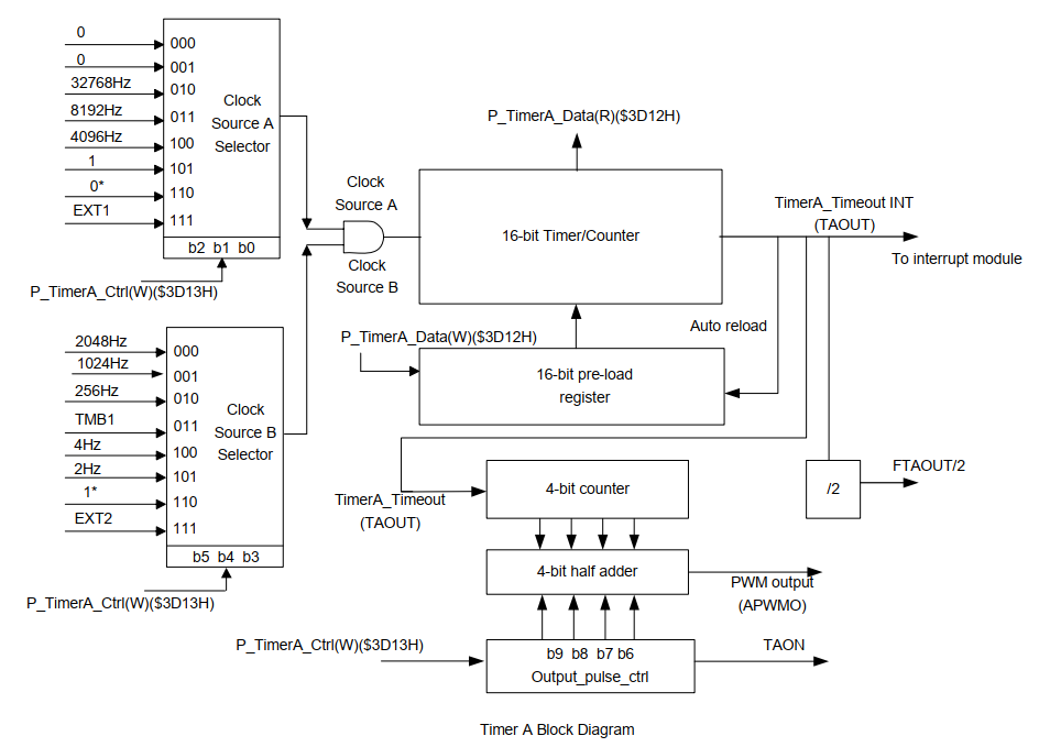
| 3D12 | TimerA Data |
| 3D13 | TimerA Control: output_pulse_ctrl (bits 9-6), source B select bits (5-3), source A select bits (2-0) |
| 3D14 | TimerA enable (bit 0) |
| 3D15 | TimerA IRQ clear (bit 0) |
| 3D16 | TimerA DATA |
| 3D17 | TimerB Control: output_pulse_ctrl (bits 9-6), source C select bits (bits 2-0) |
| 3D18 | TimerB enable (bit0) |
| 3D19 | TimerB IRQ clear (bit0) |
| 3D1C | Scanline counter |
Timebase values:
- 00: TMB2 = 128Hz, TMB1 = 8Hz
- 01: TMB2 = 256Hz, TMB1 = 16Hz
- 10: TMB2 = 512Hz, TMB1 = 32Hz
- 11: TMB2 = 1024Hz, TMB1 = 64Hz
Timer A
Timer A ticks on the rising edge of the AND of sources A and B (so one source can be used to mask the other).
The counter is incremented at each tick until it reaches FFFF and overflows.
Reading the data register allows to know the current timer value.
When the timer overflows, several things happen:
- An interrupt is triggered (if activated)
- The FTAOUT pin is toggled
- The counter is reloaded to the last value written to the data register
- The 4 bit counter for PWM generation is incremented
Control register bits 2-0: Source A
- 00x: Timer disabled
- 010: 32768Hz
- 011: 8192Hz
- 100: 4096Hz
- 101: 1 (use source B only)
- 110: Timer disabled
- 111: EXT1
Control register bits 5-3: Source B
- 000: 2048Hz
- 001: 1024Hz
- 010: 256Hz
- 011: TMB1
- 100: 4Hz
- 101: 2Hz
- 110: 1 (use source A only)
- 111: EXT2
Control register bits 9-6: output pulse control
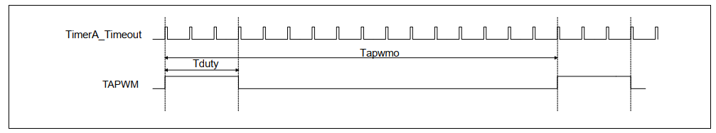
This configure the pulse width from 0 to 15 timer ticks. A new pulse starts every 16 ticks.
Misc. peripherals
| Address | Contents |
|---|---|
| 3D20 | System Control |
| 3D21 | Interrupts control |
| 3D22 | Interrupt status (read)/ clear (write) |
| 3D23 | External Memory Control |
| 3D24 | Watchdog clear (write 55AA) |
| 3D25 | ADC Control |
| 3D27 | ADC data |
| 3D28 | Sleep Mode (write AA55) |
| 3D29 | Wakeup Source |
| 3D2A | Wakeup Time |
| 3D2B | TV System (read only, bit0 indicaters NTSC or PAL) |
| 3D2C | Pseudo Random1 |
| 3D2D | Pseudo Random2 |
| 3D2E | FIQ Sel |
| 3D2F | DS register |
System control
- Bit 15: enable watchdog
- Bit 14: enable sleep
- Bit 9: Low-voltage regulator output enable
- Bit 8: Low-voltage regulator enable
- Bit 7: #2V out
- Bits 6-5: Low-voltage regulator voltage select
- Bit 4: 32KHz clock
- Bit 2: Video DAC enable
- Bit 1: Audio DAC enable
Interrupts
The three interrupt registers have the same layout:
- Bit 13: ADC (interrupt vector is at FFFB)
- Bit 12: External interrupt 2 (FFFD)
- Bit 11: Timer A (FFFA)
- Bit 10: Timer B (FFFA)
- Bit 9: External interrupt 1 (FFFD)
- Bit 8: UART (FFFB)
- Bit 7: Key change (FFFF)
- Bit 6: 4096Hz (FFFE)
- Bit 5: 2048Hz (FFFE)
- Bit 4: 1024Hz (FFFE)
- Bit 3: 4Hz (FFFF)
- Bit 1: TMB1 (FFFF)
- Bit 0: TMB2 (FFFF)
There are interrupts coming from devices, which have separate enable bits in each of the devices.
The complete list of interrupt vectors is:
| Vector address | Name | Triggered by |
|---|---|---|
| FFF5 | BREAK | break CPU instruction |
| FFF6 | FIQ | configured by 3D2E |
| FFF7 | RESET | Console startup/reset |
| FFF8 | IRQ0 | PPU |
| FFF9 | IRQ1 | SPU |
| FFFA | IRQ2 | Timers A and B |
| FFFB | IRQ3 | UART, SPI, SIO, I2C |
| FFFC | IRQ4 | SPU beat and envelope |
| FFFD | IRQ5 | External interrupts |
| FFFE | IRQ6 | 1024, 2048 or 4096Hz ticker |
| FFFF | IRQ7 | 4Hz ticker, TMB1, TMB2, LVD, Key change |
As the vector addresses are only 16-bit, they can only point to the first segment (0x0000 - 0xFFFF).
External bus configuration
- Bits 11-8: Ram decode control
- Bits 7-6: Address decode control
- Bits 5-3: Bus arbitration control
- Bits 2-1: Number of wait states
- Bit 0: CKOEN
ADC
Control register:
- Bit 13: interrupt status
- Bit 12: request conversion
- Bit 10: auto request
- Bit 9: interrupt enable
- Bit 8: VRT enable
- Bits 5-4: select channel
- Bits 3-2: clock select
- Bit 1: CSB
- Bit 0: ADE
Sleep/Wakeup
Wakeup source:
- Wakeup source: same layout as the interrupt registers, but only the 8 low bits are available?
- Wakeup time: number of 32kHz clock cycles (8 bits)
- Sleep: write AA55 here to start sleeping. CPU will be halted until the next wakeup event.
Pseudo random generators
There are two generators using the formula f(x) = x^15+x^14+1.
The first one has a default seed = 001_0100_0001_1000 The second one has a default seed = 001_0110_0101_1000
You can write the registers to set a new seed.
FIQ
There can only be a single FIQ source active at a time. This register selects which one.
- 000: PPU
- 001: SPU
- 010: TimerA
- 011: TimerB
- 100: UART(SPI)
- 101: External
- 110: ADC
- 111: None
DS register
This allows direct read and write access to the DS (Data Segment) register. Normally in the uN'SP architecture, this register is part of the CPU SR register. However, this makes it unconvenient to change its value. This memory mapped version of the register can be used with usual CPU instructions to set and use the DS value more conveniently.
UART
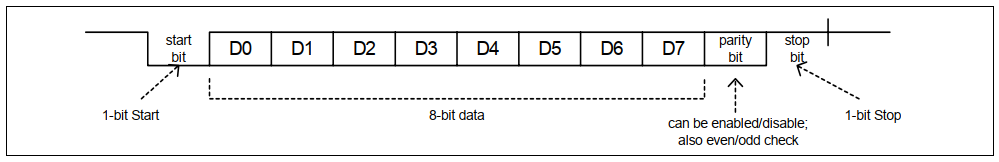
All UART registers are 8bit only.
| Address | Contents |
|---|---|
| 3D30 | UART Control (7: TxEn, 6: RxEn, 5: Mode, 4: MulPro, 3-2: bits per byte, 1: Tx Interrupt Enable, 0: Rx Interrupt Enable |
| 3D31 | UART Status (7: Rx buffer full, 6: Tx busy, 5: bit9, 4: overrun, 3: frame error, 2: parity, 1: tx ready, 0: rx ready |
| 3D32 | UART Reset (bit 0) |
| 3D33 | UART Baudrate setting (low byte) |
| 3D34 | UART Baudrate setting (high byte) |
| 3D35 | UART Tx buffer |
| 3D36 | UART Rx buffer |
Baudrate settings:
- 1200: FA 92
- 2400: FD 41
- 4800: FE A0
- 9600: FF 50
- 19200: FF A8
- 57600: FF E2
- 115200: FF F1
SPI
| Address | Contents |
|---|---|
| 3D40 | SPI Control (bit 8: busy, bit 7: tx empty, bit 6: rx full, bit 5: SPH, bit 4: SPO, bit 3: SPIEN, bit 2: LPM, bit 1: Tx Interrupt Enable, bit 0: Rx Interrupt Enable) |
| 3D41 | SPI Data (write to send, read to receive) |
| 3D42 |
General DMA
| Address | Contents |
|---|---|
| 3E00 | DMA Source address |
| 3E01 | DMA Source segment |
| 3E02 | DMA word count |
| 3E03 | DMA Target Address (14 bits) |
This is a DMA for generic purposes. Note that there is another DMA channel in the PPU registers.
Both DMA units operate in the same way. First, set the source and destination addresses. The source can be anywhere in memory, but the destination register is only 14 bits wide, which allows to target only the internal RAM and IO registers (you wouldn't write to ROM, would you?).
The transfer is started when you write the word count register, and you can read that register to know when the transfer is done (the register is 0 when there are no more words to transfer).
