Table of Contents
Cartridge port
50 pin connector with spacing of 2.54mm. For example this works: https://www.digikey.com/product-detail/en/te-connectivity-amp-connectors/5530841-5/5530841-5-ND/2259225
One pair of pins is missing, making a hole that prevents inserting cartridges in the wrong way.
V.Smile cartridges
Pinout traced from development cart picture: https://media.discordapp.net/attachments/750094909947772964/758513072087629884/vsmile-pinout.png?width=1011&height=684
Development cartridges from V.Tech used NOR flash memory: SST 39VF6401B (4Mx16 flash memory). The write pin is exposed on the cartridge port, so in theory it's possible to reflash it directly from the console?
Production cartridges use a “blob” and it's unknown what exactly is under it. Probably mask ROM.
| Pin N | 1 | 2 | 3 | 4 | 5 | 6 | 7 | 8 | 9 | 10 | 11 | 12 | 13 | 14 | 15 | 16 | 17 | 18 | 19 | 20 | 21 | 22 | 23 | 24 | 25 |
|---|---|---|---|---|---|---|---|---|---|---|---|---|---|---|---|---|---|---|---|---|---|---|---|---|---|
| Front | /WE | /OE | GND | D3 | D4 | D5 | D6 | D11 | D12 | D13 | D15 | A0 | A1 | A3 | x | A5 | A7 | A18 | A9 | A11 | A13 | A15 | A20 | GND | Card detect |
| Back | VDD | RAM CSB | Sense | ROM CSB2 | D2 | D1 | D0 | D7 | D10 | D9 | D8 | D14 | A16 | A2 | x | A4 | A6 | A17 | A8 | A10 | A12 | A14 | A19 | A21 | ROM CSB1 |
Note: the “back” side is the one with the label. Chips inside the cartridge are on the side with no label.
- Sense is connected to VDD to indicate that a cart is inserted. It is connected to the RESET pin, so inserting a cartridge will power the console off.
- Card detect is connected to VDD to indicate that a cart with ROM is inserted (?) maybe it allows booting from cartridge instead of internal ROM (tbc)
- ROM CSB1, ROM CSB2 and RAM CSB allow to select which bank of the cartridge is accessed. Typically cartridges use only ROM CSB1, but larger cartridges (example: alphabet adventure) need two ROM banks. ROM_CSB2 may also be used for battery-backed SRAM. The two pins are controlled independently as GPIO from the CPU, so all 4 combinations are possible. However, 11 will be used when the internal ROM is accessed, so it's better to have the cartridge idle in that case.
To be confirmed:
- What is RAM_CSB? It is not connected on the only cart known to use SRAM. The name of the pin comes from schematics of the console but it just shows that it is connected to the SPG200C without any other info. SPCE1600 datasheet shows it would be usable for external RAM, where in the address space would it be mapped in that case?
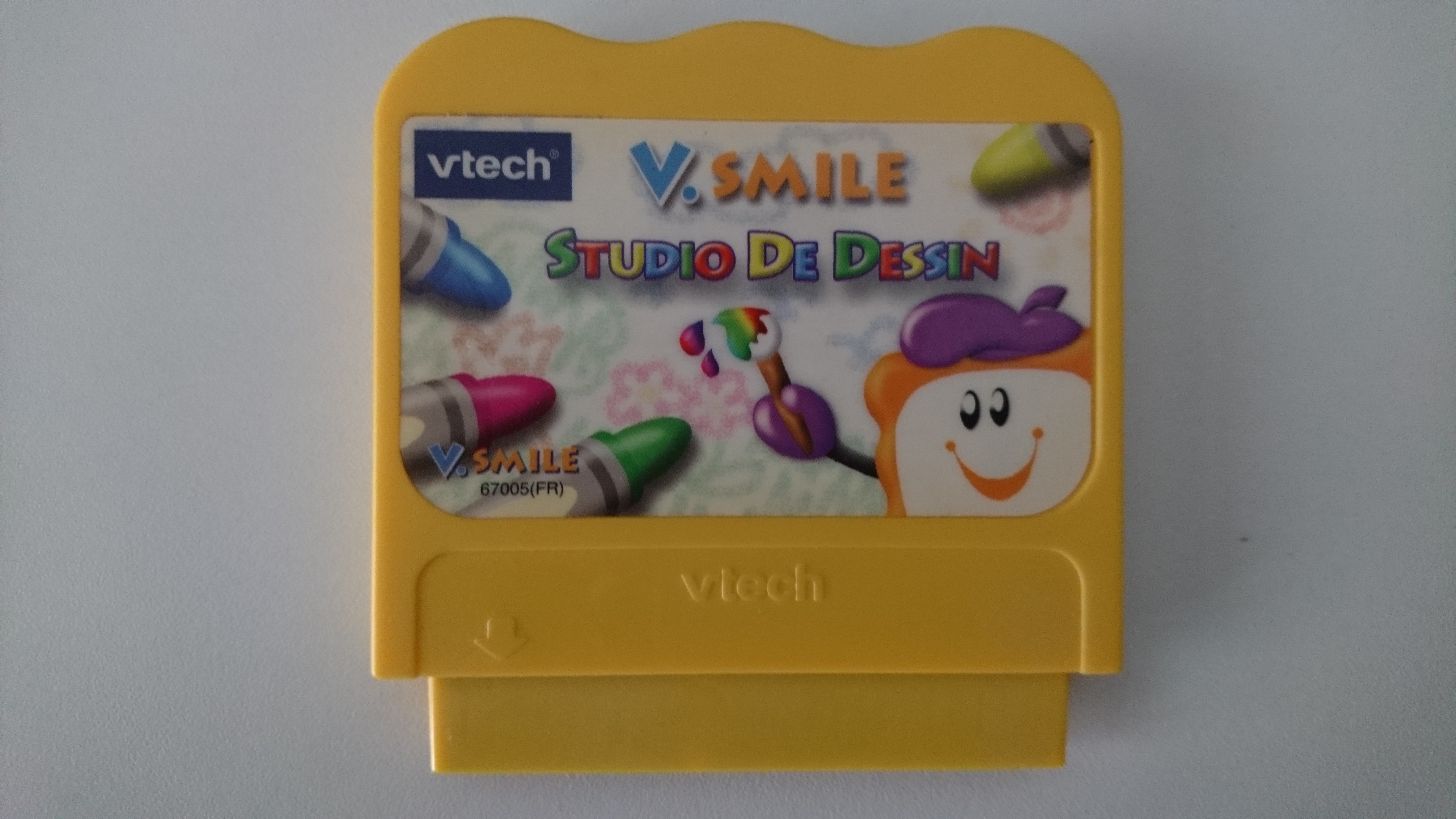
Battery backup cartridge
At least the “Studio de Dessin” cartridge (the one for the graphic tablet) has backup SRAM
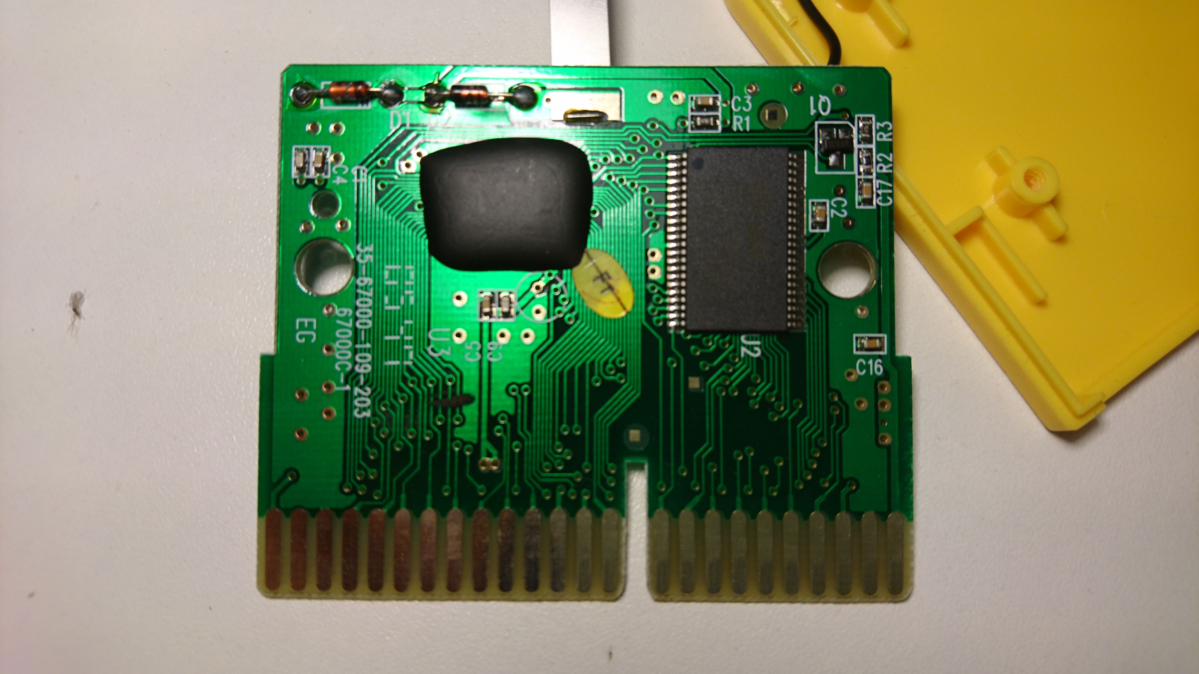
The blob is flash (as usual) and the chip on the right is RAM: BSI - BS616LV2016ECG70 - S31688EB04308B1 - E05162 - Taiwan
The pin labelled RAM_CSB in the pinout above is in fact not used by this cartridge (but ROM_CSB2 is)
Dual ROM cartridges
At least the following games have two blobs on ROM_CSB1 and ROM_CSB2:
- The little mermaid
- Smart keyboard
- Alphabet adventure
Nitro Vision / Genius TV progress cartridges
These contain no ROM, and only short some pins together.
Inserting these in the V.Smile results in nothing special (the boot animation loops as if there was no cartridge). However the SENSE pin is there, so they still power the console off if connected while it is on.
| Cartridge name | Number (marked on PCB) | Shorted pins |
|---|---|---|
| Français et Anglais (orange) | 1 - 35-68700-017-202-707426-1 | SENSE is connected to VDD |
| Sciences et Nature (white) | 2 - 35-68700-018-202-707427-1 | SENSE and RAM_CSB are connected to VDD |
| Découvre le monde (blue) | 3 - 35-68700-019-202-707428-1 | SENSE and ROM_CSB2 are connected to VDD |
| Maths et Logique (green) | 4 - 35-68700-020-202-707429-1 | SENSE, RAM_CSB and ROM_CSB2 are connected to VDD |
So, in this case:
- Sense indicate that a cartridge is inserted
- RAM_CSB and ROM_CSB2 allow to identify which cartridge it is
